
How is the Layout of an RF Board Optimized?
Layout of an RF Board
The layout of an RF board is different from traditional PCBs, as it requires special considerations to maximize signal transmission and minimize interference. This includes factors like trace width and spacing, impedance matching, and more. By utilizing these techniques, an RF board can achieve optimal performance.
An RF board must be designed using an appropriate copper thickness to reduce skin effect and ensure proper conductivity. In addition, the copper material should be selected based on its dielectric constant and thermal properties. In particular, a high-frequency signal will generate substantial heat in its path. The thermal characteristics of the material will play an important role in preventing the soldering process from deforming the board and causing signal loss.
RF circuits are also more prone to electromagnetic interference (EMI) and crosstalk, so the layout must be carefully designed. The distance between traces and the size of their bend radius must be appropriate for reducing these effects. The choice of component placement and the layout of traces are also critical for improving EMI performance.
A key feature of an rf board is its characteristic impedance, which determines how much power it can transfer without distortion. This impedance is determined by several factors, including the geometry of the trace, the dielectric constant of the PCB material, and the track thickness. An RF circuit can only operate at its rated frequency if the impedance is the same throughout its length. This is why RF trace lengths should be as short as possible.
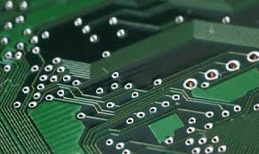
How is the Layout of an RF Board Optimized?
Another important aspect of a RF PCB is the routing of its power and ground planes. It is recommended to place these on separate layers and avoid routing RF signals between them, as this can cause unwanted coupling and increase noise. It is also crucial to use adequate decoupling capacitors, which will filter out low-frequency noise and prevent the current from leaking through the circuit board.
It is also a good idea to route the VCC lines on their own layer. This will ensure that they receive sufficient decoupling, reducing their own noise and voltage drops. In addition, it is recommended to use larger bend radii for these lines.
The RF signals should be routed on the top layer of the board. This will allow them to have a shorter return path, resulting in less attenuation. It is also recommended to use stitching vias for routing RF signals between layers. These offer a smaller footprint and better impedance matching than regular vias.
It is important to keep in mind that RF traces are transmission lines, so they must be as straight as possible to minimize attenuation and interference. This can be difficult, as many traces are required for high-speed digital components and RF signaling. However, there are a few things that can be done to make sure that these lines are as straight as possible: Keep the traces as short as possible. Avoid any abrupt changes in line width or direction. Reduce the number of holes drilled for these signals, and add more ground vias.